Beyond the Silicon: How Nvidia''s Grip on TSMC''s CoWoS Packaging is Reshaping
The AI chip boom has exposed a critical bottleneck beyond transistor fabrication:
Beyond the Silicon: How Nvidia's Grip on TSMC's CoWoS Packaging is Reshaping the AI Chip Supply Chain
The narrative of semiconductor progress has long been dominated by the race for transistor miniaturization. However, the explosive demand for artificial intelligence compute has exposed a critical, less-visible constraint. The primary bottleneck for leading AI accelerators is no longer solely the fabrication of transistors but the advanced packaging required to interconnect them. At the center of this constraint is TSMC’s CoWoS (Chip-on-Wafer-on-Substrate) technology, a capacity pool for which Nvidia has secured a dominant share for 2024 and 2025 (Source 1: [Primary Data]). This move signals a fundamental shift in the semiconductor competitive landscape, where control over the manufacturing stack is becoming as strategically vital as chip design.
The Hidden Bottleneck: Why Packaging, Not Just Fabrication, is Choking AI Progress
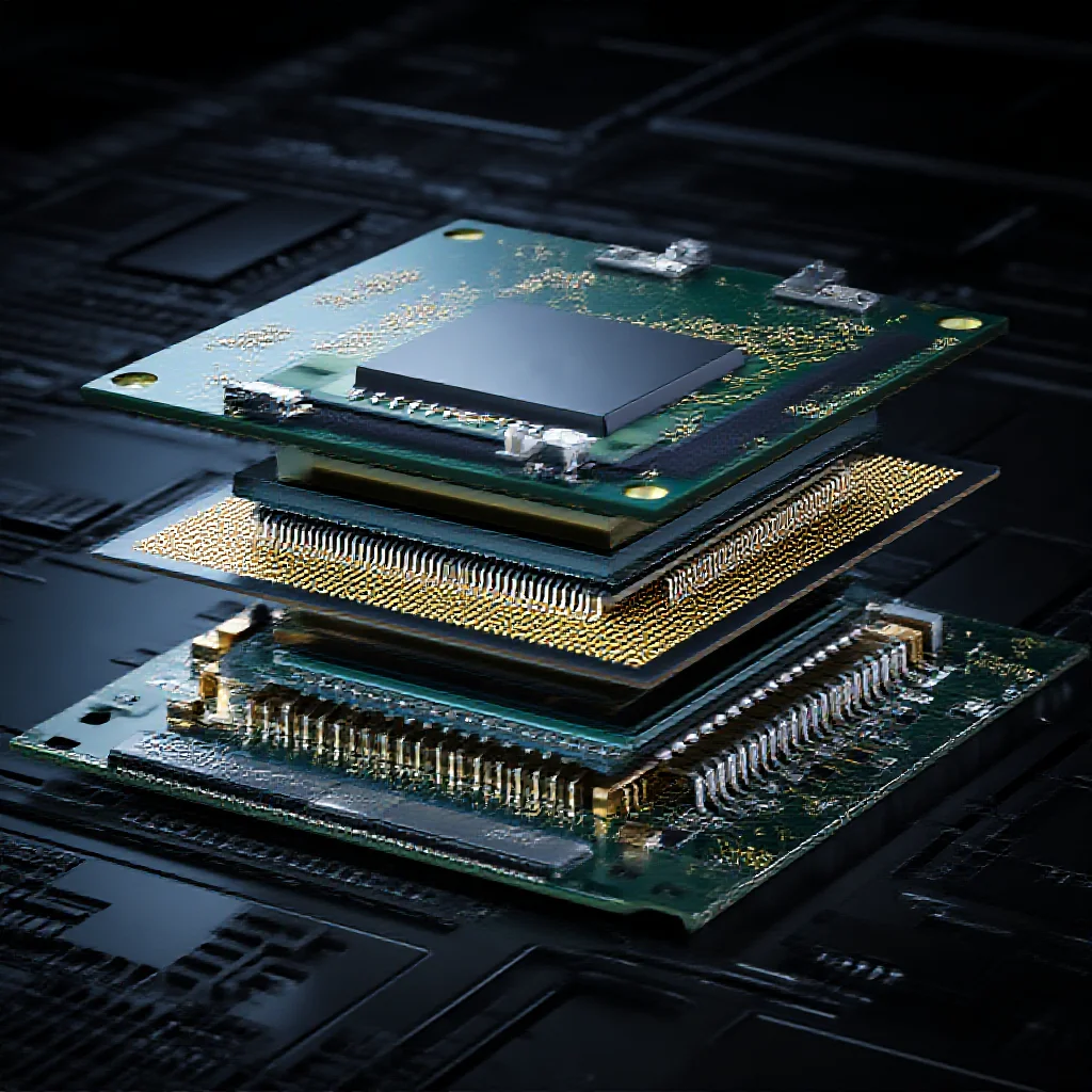
While Moore's Law focuses on transistor density, the performance of modern AI chips is equally dependent on memory bandwidth. Technologies like CoWoS enable the direct, high-density integration of multiple processor chiplets and stacks of High-Bandwidth Memory (HBM) onto a single substrate. This architecture is the foundation of chips like Nvidia's H100 and its successors, allowing for the massive data throughput required for large language model training. The industry's focus has now pivoted from the front-end process of etching transistors to the back-end challenge of assembling these complex systems-in-package. The scarcity of advanced packaging capacity is directly limiting the supply of AI chips (Source 2: [Primary Data]). This marks a strategic inflection point: competitive advantage is migrating from architectural design prowess alone to the ability to secure and control the entire physical realization of the chip.
Nvidia's Strategic Lock: More Than Just Supply Security
Nvidia’s pre-booking of a large portion of TSMC’s CoWoS capacity is a multifaceted strategic maneuver. Primarily, it guarantees the production scale necessary to meet its own forecasted demand, securing its growth trajectory. Secondarily, it functions as a defensive moat. Competitors, including AMD and a growing cohort of companies developing custom AI silicon, rely on the same finite pool of TSMC’s advanced packaging resources. By securing capacity for 2024 and 2025 (Source 1: [Primary Data]), Nvidia potentially constrains the market’s ability to scale viable alternatives in the near term. This dynamic alters the traditional fabless-foundry relationship, granting Nvidia significant leverage in partnership negotiations and priority access, thereby blurring the lines between customer and strategic stakeholder.
TSMC's Double-Edged Sword: Capacity Expansion and Dependency
The foundry’s response to this bottleneck is a massive scaling effort. TSMC has announced plans to double its CoWoS packaging capacity by the end of 2024 (Source 3: [Primary Data]). This expansion is a direct reaction to overwhelming market demand and reinforces TSMC’s position as the indispensable enabler of cutting-edge AI hardware. However, this move carries inherent risks. The capital expenditure required for specialized packaging capacity is substantial and must be deployed with precision to match a market whose long-term growth trajectory remains to be fully charted. Furthermore, by scaling capacity to serve a market currently dominated by one primary customer, TSMC deepens its dependency on Nvidia’s fortunes. This concentration creates vulnerability to demand volatility and increases the strategic importance of managing this key relationship.
The Ripple Effect: Long-Term Implications for the AI Ecosystem
The CoWoS capacity constraint is generating systemic effects across the AI hardware industry. For challengers, limited access to advanced packaging elongates development cycles and raises barriers to entry, potentially cementing the incumbent’s architectural and software ecosystem advantages for a longer period. This bottleneck is forcing a re-evaluation of the entire hardware stack, prompting investment in alternative packaging architectures, such as Intel’s EMIB and Foveros, and renewed interest in monolithic die designs where feasible. The situation also accelerates vertical integration strategies, with larger players likely to invest in or directly secure packaging assets. For the broader market, the determinant of who can scale AI compute is shifting from flops-per-chip to units-shipped, with packaging yield and capacity emerging as key metrics.
The industry trajectory suggests that advanced packaging will remain a critical chokepoint for the foreseeable future. While TSMC’s capacity expansion will alleviate the acute shortage, the strategic pre-commitment of that capacity by leading players indicates that market allocation, not just technical capability, will dictate the pace of innovation. The semiconductor competitive landscape is being reshaped, with the back-end packaging facility gaining parity with the front-end fab as a locus of strategic power and investment.